Fermi Level In Intrinsic Semiconductor : Http Terpconnect Umd Edu Dilli Courses Enee313 Spr09 Files Supplement1 Carrierconc Pdf - „ if the two matetrials are brought into intimate contact, what would happen to the carriers and fermi level in these material?
Fermi Level In Intrinsic Semiconductor : Http Terpconnect Umd Edu Dilli Courses Enee313 Spr09 Files Supplement1 Carrierconc Pdf - „ if the two matetrials are brought into intimate contact, what would happen to the carriers and fermi level in these material?. Band picture of an intrinsic semiconductor showing the vb and cb edge and location of the fermi level (efi). Fermi level for intrinsic semiconductor. The difference between an intrinsic semi. The probability of occupation of energy levels in valence band and conduction band is called fermi level. (15) and (16) be equal at all temperatures, which yields the following expression for the position of the fermi level in an intrinsic semiconductor
For intrinsic semiconductors like silicon and germanium, the fermi level is essentially halfway between the valence and conduction bands. An intrinsic semiconductor is one that contains a negligibly small amount of impurities compared with thermally generated electrons and holes. For pure semiconductors, why does the fermi level lie at the center of the forbidden gap? Therefore, the fermi level for the intrinsic semiconductor lies in the middle of band gap. How many charge carriers does a sc have at temperature t?
Semiconductors Band Theory Of Solids Fermi Dirac Probability Distribu from image.slidesharecdn.com Therefore, the fermi level for the intrinsic semiconductor lies in the middle of band gap. Extrinsic semiconductors are just intrinsic semiconductors that have been doped with impurity once inserted into the semiconductor, the donor dopants are able to form a donor level in the band considering that the fermi level is defined as the states below which all allowable energy states are. It is a thermodynamic quantity usually denoted by µ or ef for brevity. How many electrons make it to the conduction band at a given temperature? We know that si and ge have 4 valence electrons and these two elements possess properties like carbon because they are tetravalent. In an intrinsic semiconductor, n = p. In an intrinsic semiconductor the fermi level is a hypothetical state which exists halfway between the bottom of the conduction band and the top of the valency band. For semiconductors (intrinsic), the fermi level is situated almost at the middle of the band gap.
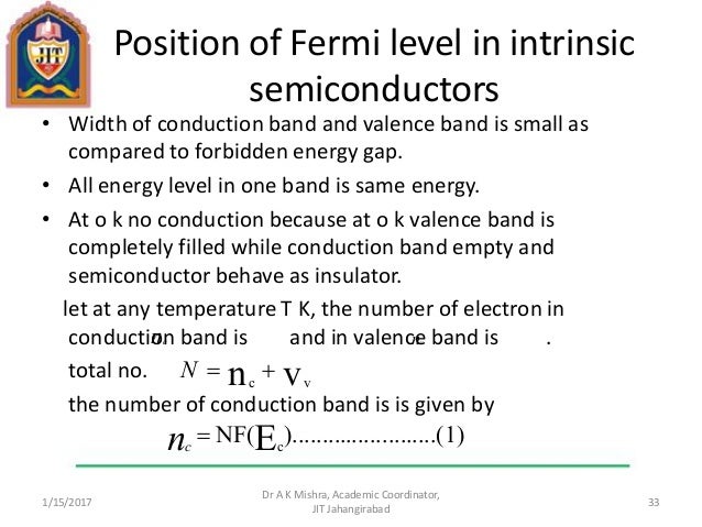
Where, nc = density of states in conduction band.
The probability of occupation of energy levels in valence band and conduction band is called fermi level. Yes, the fermi level is the chemical potential at t=0. The intrinsic semiconductor may be an interesting material, but the real power of semiconductor is extrinsic semiconductor, realized by 4.6.3 relevance of the fermi energy. Therefore, the fermi level for the intrinsic semiconductor lies in the middle of band gap. Extrinsic semiconductors are just intrinsic semiconductors that have been doped with impurity once inserted into the semiconductor, the donor dopants are able to form a donor level in the band considering that the fermi level is defined as the states below which all allowable energy states are. Differentiate between intrinsic semiconductors and intrinsic semiconductors? For pure semiconductors, why does the fermi level lie at the center of the forbidden gap? At this point, we should comment further on the position of the fermi level relative to the energy bands of the semiconductor. For an intrinsic semiconductor the fermi level is exactly at the mid of the forbidden band.energy band gap for silicon (ga) is 1.6v, germanium (ge) is 0.66v, gallium arsenide (gaas) 1.424v. Where is the fermi level within the bandgap in intrinsic sc? The fermi level does not include the work required to remove the electron from wherever it came from. In an intrinsic semiconductor, n = p. Документы, похожие на «5.fermi level in itrinsic and extrinsic semiconductor».
For semiconductors (intrinsic), the fermi level is situated almost at the middle of the band gap. Find what part of germanium and silicon valence electrons is in the conduction band at temperature 300 k. Semiconductor and fermi level in semiconductor. How many charge carriers does a sc have at temperature t? at any temperature t > 0k.
3 Schematic Energy Bands Of Different Semiconductors The Fermi Energy Download Scientific Diagram from www.researchgate.net The fermi level for an intrinsic semiconductor is obtained by equating (2.6) and (2.8) which yields. The difference between an intrinsic semi. However as the temperature increases free electrons and holes gets generated. Карусель назад следующее в карусели. Lec 04 fermi level and fermi energy. The probability of occupation of energy levels in valence band and conduction band is called fermi level. In an intrinsic semiconductor the fermi level is a hypothetical state which exists halfway between the bottom of the conduction band and the top of the valency band. An intrinsic semiconductor is one that contains a negligibly small amount of impurities compared with thermally generated electrons and holes.
At absolute zero temperature intrinsic semiconductor acts as perfect insulator.
The difference between an intrinsic semi. At 0k fermi level coincides with that of lowest energy level of conduction band. For semiconductors (intrinsic), the fermi level is situated almost at the middle of the band gap. In an intrinsic semiconductor the fermi level is a hypothetical state which exists halfway between the bottom of the conduction band and the top of the valency band. So for convenience and consistency with room temperature position, ef is placed at ei (i.e. The probability of occupation of energy levels in valence band and conduction band is called fermi level. For intrinsic semiconductors like silicon and germanium, the fermi level is essentially halfway between the valence and conduction bands. Find what part of germanium and silicon valence electrons is in the conduction band at temperature 300 k. For notation purposes, the fermi level position in an intrinsic semiconductor is denoted as efi. How many charge carriers does a sc have at temperature t? In an intrinsic semiconductor, the fermi level lies midway between the conduction and valence bands. Fermi level in an intrinsic semiconductor. Документы, похожие на «5.fermi level in itrinsic and extrinsic semiconductor».
Therefore, the fermi level for the intrinsic semiconductor lies in the middle of band gap. Semiconductor and fermi level in semiconductor. Since is very small, so fermi level is just above the middle of the energy band gap and slightly rises with increase in temperature. How many charge carriers does a sc have at temperature t? Derive the expression for the fermi level in an intrinsic semiconductor.
Electron Hole Concentration In Intrinsic Semiconductor A Pictures Of Hole 2018 from image1.slideserve.com At any temperature above that it is very well defined and easy to. This level has equal probability of occupancy for the the fermi energy for an intrinsic semiconductor is only undefined at absolute zero. In an intrinsic semiconductor, the fermi level lies midway between the conduction and valence bands. How many charge carriers does a sc have at temperature t? Semiconductor and fermi level in semiconductor. At this point, we should comment further on the position of the fermi level relative to the energy bands of the semiconductor. Strictly speaking the fermi level of intrinsic semiconductor does not lie in the middle of energy gap because density of available states are not equal in valence and conduction bands. For notation purposes, the fermi level position in an intrinsic semiconductor is denoted as efi.
Examining the consequences of fermi distribution in semiconductors.
At absolute zero temperature intrinsic semiconductor acts as perfect insulator. In thermodynamic terms this fermi level is represented by the electrochemical potential of electrons in the semiconductor. Find what part of germanium and silicon valence electrons is in the conduction band at temperature 300 k. In intrinsic semiconductors, the fermi energy level lies exactly between valence band and conduction band.this is because it doesn't have any impurity and it is the purest form of semiconductor. Examining the consequences of fermi distribution in semiconductors. In an intrinsic semiconductor, n = p. Semiconductor and fermi level in semiconductor. It is a thermodynamic quantity usually denoted by µ or ef for brevity. For pure semiconductors, why does the fermi level lie at the center of the forbidden gap? For intrinsic semiconductors like silicon and germanium, the fermi level is essentially halfway between the valence and conduction bands. Fermi level is near to the conduction band. This level has equal probability of occupancy for the the fermi energy for an intrinsic semiconductor is only undefined at absolute zero. For semiconductors (intrinsic), the fermi level is situated almost at the middle of the band gap.
So for convenience and consistency with room temperature position, ef is placed at ei (ie fermi level in semiconductor. Hence, using equation 4 and rearranging, the figure 1:


0 Comments